SF State researchers use lasers, gold to test super-thin materials

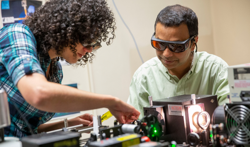
SF State graduate student Viviane Costa (left) and Physics & Astronomy Professor AKM Newaz adjust a microscope in the lab.
Single-layer semiconductors could lead to advances in miniaturization
As technologies become more compact — with the room-sized computers of the past shrinking to smartphones as just one example — you eventually reach a limit. In a new study, San Francisco State University scientists push against that limit, probing the properties of a futuristic material made up of just a single layer of molecules. The team used lasers, vaporized gold and even employed some strategic sticky tape to gain a better understanding of the material, which may one day allow for extreme miniaturization of technologies like lasers and LED lights.
San Francisco State Assistant Professor of Physics & Astronomy AKM Newaz started digging into the material molybdenum disulfide (or MoS2 for short) in 2016. He was intrigued by its ability to be created a single molecule thick — nearly 100,000 times thinner than a human hair. It’s also a semiconductor, a class of materials that play a crucial role in computers because of their ability to alter electric currents.
The same trait that gives MoS2 its interesting properties also makes it difficult to work with. To test the material in the way it would actually be used in next-generation technologies it needs to be sandwiched between metals, but the typical process for doing so involves placing it on a gold surface that has hills and valleys that would bend the material out of shape. “You’re putting a blanket on a mountain,” Newaz explained. The resulting curvature makes it impossible to accurately measure the material’s properties.
One breakthrough in the recent study by Newaz and his lab members was a new way around that. The technique they developed involved evaporating gold onto a flat surface with super-hot temperatures, sticking a flat sheet of silicon wafer on the condensed molten metal and then peeling it off. The resulting, far smoother gold surface allowed the scientists to mount the MoS2 on it using sticky tape — a must-have in any lab studying ultra-thin materials — while keeping its properties intact. “That was one of the most important things in this work: We found a way to make this ultra-flat gold surface,” Newaz said.
The next step was passing an instrument with a tiny metal tip paired with a laser over the material to map out its physical peaks and valleys. “It senses the ups and downs, like reading Braille,” Newaz explained. Combining that with measurements of electric current let the team measure MoS2’s electric characteristics and how those characteristics change when layers of the material are stacked on top of one another.
Using a similar setup with a transparent metal, they then measured the material’s “opto-electric” behavior — how light influences electric current. That led to a surprising discovery: Shining a laser on the material, rather than increasing the electricity flowing through it, makes the electric current running through MoS2 decrease, a rare property called negative photoconductivity. They published the results of their work in the journal ACS Applied Materials and Interfaces on Aug. 19, with graduate student Hao Lee (M.S., 2019), now an alumnus, as lead author.
It’s not yet clear how these properties will translate in terms of the material’s eventual usefulness, but the study is an important first step towards finding uses for ultraflat materials, Newaz says. One area Newaz sees MoS2 being useful is in translating electric signals to light signals, something a computer does whenever it sends data into a fiber-optic cable. “You need to have a very efficient switching circuit,” Newaz explained. “Currently this is one of the bottlenecks in the technology — your efficiency isn’t super high.”
The team’s next step will be figuring out why the material behaves the way it does, performing similar tests with a variety of different colors of light and under temperatures down to just a few degrees above absolute zero.